USRP Diagrams - mux usage
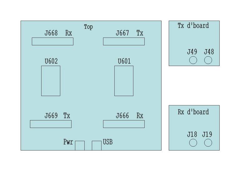
Board layout of ADC/DAC's and connectors:
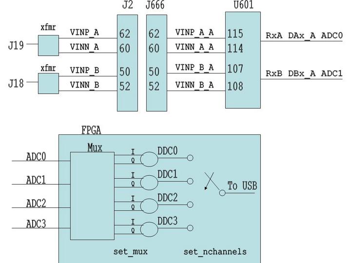
Rough signal path from SMA sockets on right side basic RX
board thru the ADC, FPGA to the USB bus:
From usrp_standard.h:
  /*!
   * \brief Set input mux configuration.
   *
   * This determines which ADC (or constant zero) is connected to
   * each DDC input.  There are 4 DDCs.  Each has two inputs.
   *
   *
   * Mux value:
   *
   *    3                   2                   1
   *  1 0 9 8 7 6 5 4 3 2 1 0 9 8 7 6 5 4 3 2 1 0 9 8 7 6 5 4 3 2 1 0
   * +-------+-------+-------+-------+-------+-------+-------+-------+
   * |   Q3  |   I3  |   Q2  |   I2  |   Q1  |   I1  |   Q0  |   I0  |
   * +-------+-------+-------+-------+-------+-------+-------+-------+
   *
   * Each 4-bit I field is either 0,1,2,3
   * Each 4-bit Q field is either 0,1,2,3 or 0xf (input is const zero)
   * All Q's must be 0xf or none of them may be 0xf
   *
   */
  bool set_mux  (int mux);
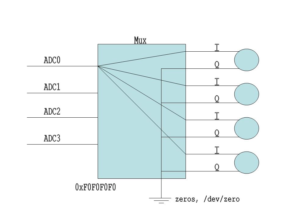
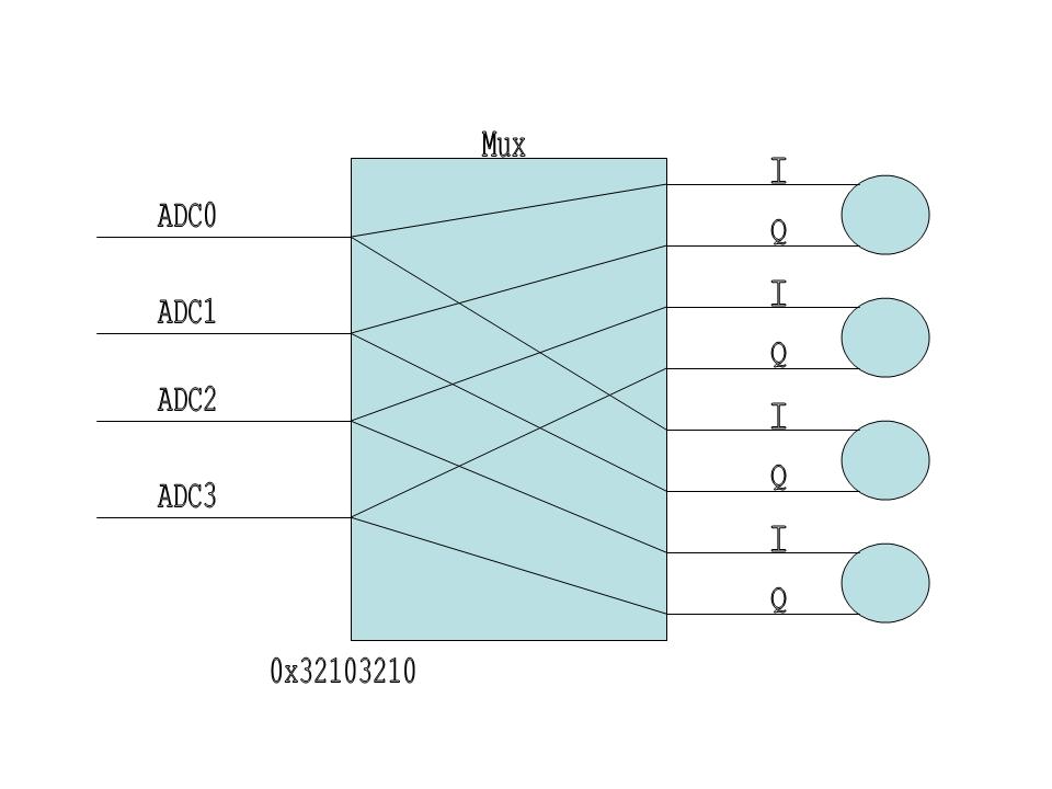
The receive side multiplexer allows you to connect any of the 4 analog
digital converters (ADC0 thru ADC3) to any of the digital down-converters
(DDC0 thru DDC3) I or Q input. That's 4-in, 8-out. Also, you can short
all the DDC Q inputs to ground (zeros). More on the DDC's later. The mux
parameter is 32 bits, each nybble of 4 bits controls which ADC is connected
to which DDC input.
Common examples: 0xF0F0F0F0 sends constant zeros
to each Q input, and ACD0, which digitizes the signal from J19, goes
to the I inputs of each DDC. If nchannels
is 1, you get the digitized data of the signal connected to J19.
0xF0F0F0F1 is
the same except now J18, thru ADC1, goes to DDC0 and to the software.
Going to the other side of the USRP, 0xF0F0F0F2 sends the signal from J19
on the daughterboard plugged into J668 to DDC0, and 0xF0F0F0F3 would send
the signal from J18 to DDC0. An oddball example, 0xF2F2F0F1 would still
ground all Q inputs, send J19 on the left side to DDC2 & 3, J19 on the
right side to DDC1 and J18 on the right side to DDC0.
Another example:
0x32103210 connects J18 on the left to DDC3 Q input, J19 on the left
to DDC3 I input, right J19 DDC2 Q input, right J18 to the
DDC2 I input, left J19 to DDC1 Q input, left J18 to the DDC1 I input,
right J19 to DDC0 Q input and right J18 to DDC0 I input.
How is data from the different DDC's accessed? They are interleaved
across the USB bus according to the setting of nchannels. Again
from usrp_standard.h:
  /*!
   * \brief Set number of active channels.  \p nchannels must be 1, 2 or 4.
   *
   * The final complex sample rate across the USB is
   *   adc_freq () / decim_rate () * nchannels ()
   */
  bool set_nchannels (int nchannels);
When set to 1, you only get a complex stream from DDC0. When 2, you get
DDC0 / DDC1 / DDC0 / DDC1 etec. 4 interleaves all DDC's. You separate
the streams out in software using something like gr.stream_to_streams().
More on the Digital Down-Converters (1st mixer for us old-timers):
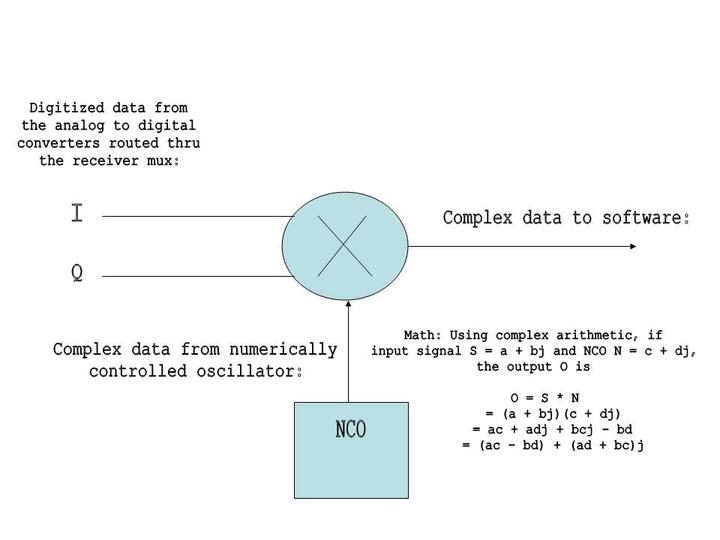
where j = sqr(-1). When the Q input gets constant zeros, b=0 and the math simplifies to
O = ac + adj, which is why we still get a stream of complex, quadrature data from
the DDC when digitizing only one input signal.